Nanowatts Scientific Laboratory ISO ACCREDITED Services
Materials Testing and Characterization
Consumer Product Testing and Quality Assurance
Materials Testing and Characterization
Insights into the properties, and performance of your materials by
- Electron microscopy lab (SEM, TEM, FIB, AFM)
- Molecular and chemical analysis (FTIR, Raman, TGA)
- Chemical material analysis (XRD, XPS, XRF)
- Surface, morphology, and defect characterization

Nanofabrication and Microelectronics
Consumer Product Testing and Quality Assurance
Materials Testing and Characterization
From concept to prototype, we provide expertise to support your micro and nanotechnology projects.
- Nanofabrication facilities including lithography, etch, Deposition and packaging.
- Assistance with design, mask making & prototyping services.
- Development of process, device integration and packaging.

Consumer Product Testing and Quality Assurance
Consumer Product Testing and Quality Assurance
Consumer Product Testing and Quality Assurance
Helping you to improve, and validate your products with scientific precision to meet industry standards and expectations.
- Serving industries in electronics, automotive, medical devices, paint & raw materials.
- Failure analysis and root cause study services.
- Product quality assurance.
- Consumer product inspection.
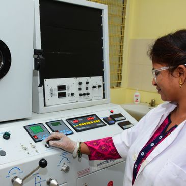
Our Lab and Testing Facilities
Our Lab and Testing Facilities
Consumer Product Testing and Quality Assurance
Our innovative facilities boast modern equipment and technology specifically tailored for nanofabrication, product inspection, nanotechnology based material testing, ensuring precise and reliable results. We provide the ideal setting for comprehensive analysis and innovation in nanomaterial research.
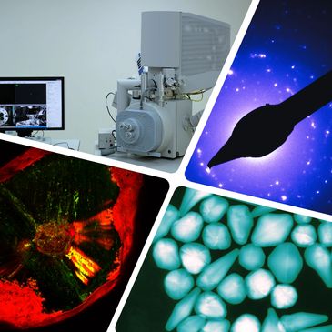
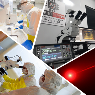
Advanced Microscopy Services
Our Lab and Testing Facilities
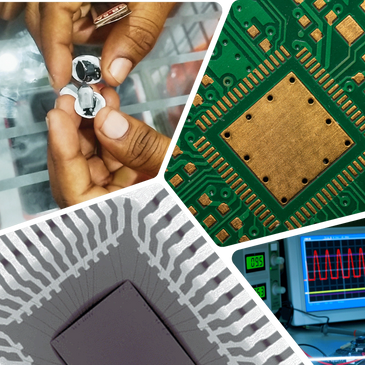
Consumer Electronics Testing
Explore the complex world of materials at the nanoscale with our advanced microscopy services, offering unparalleled resolution and precision for detailed analysis. Our instruments and expert technicians let us uncover hidden structures and properties, providing invaluable insights on your research.
Consumer Electronics Testing
Our Lab and Testing Facilities
Consumer Electronics Testing
Elevate your electronics product reliability with our comprehensive testing services, meticulously designed to ensure products to meet industry standards and exceed our customer expectations. From durability assessments to performance evaluations, our expert team delivers actionable insights to optimize products.

Our versatile scientific testing solutions
We don’t just test, we solve problems.
- Material composition XRF analysis lab
- Reverse engineering and counterfeit tests
- Mechanical and deformation study lab
- IC and PCB quality inspection lab
- Polymer and rubber materials testing lab
- ISO ASTM root cause failure
- Environmental stress & durability testing

Materials Insights & Inner Structure Analysis
- We dismantle and analyze products to understand their internal design, construction, and functionality. This helps uncover manufacturing methods and identify areas for improvement.
- Redesign and cost optimization of materials used and design choices for optimize manufacturing, reduce costs, and create smarter, more efficient next-generation products.
COMPREHENSIVE lab testing expertise

Reverse Engineering
Unlock your electronic device secrets with our flexible reverse engineering services, meticulously dissecting and analyzing products to understand their inner workings. Our expert team uses the latest techniques to reverse engineer schematics, components, and functionalities, offering valuable insights into innovation and product enhancement.
- Product purchase and product teardowns.
- Product 2D, 3D CT X-ray inspections.
- Material composition analysis and more.
Product Validation
Ensure your products reliability and market readiness with our meticulous product validation services, meticulously designed to confirm performance, safety, and compliance with industry standards. Our expert team utilizes advanced testing techniques to provide extensive validation reports, enabling you to confidently launch your products into the market.
- Product cross section inspections.
- Root cause case studies.
- In depth product analytical analysis
Quality Assessment
Gain assurance in your materials quality with our elevated quality assurance assessment services, where we evaluate and confirm your products' integrity, consistency, and reliability. Our expert team dives into advanced testing protocols and industry-leading techniques to deliver kick off assessments, ensuring your materials meet the highest quality and performance standards.
- ASTM/ISO standard tests.
- Environmental ecotoxicity assessment.
- Electromagnetic compatibility test and solutions.
Pro Visual Inspection
At Nanowatts, outsourcing services for semiconductor testing for IC's, electronic products, failure analysis, material testing & analysis, X-ray Inspection of PCB's, Bio tech services where profound attention to detail ensures the detection of even the slightest defects in your materials or products. Our expert inspectors employ advanced techniques and equipment to provide thorough assessments, providing you with confidence in the integrity and reliability of your products and materials.
- Zoom in stereo microscope services.
- Optical micro inspection solutions.
- Advanced 2D, 3D, CD/CT X-Ray inspection services.
Semiconductor Product Teardown Services

Semiconductor Die Level Analysis
- Module and multi chip packages decapsulation of SoP, PoP, BGA's, QNF & QFP die level analysis.
- Failure mode investigation of failed devices due to electrical overstress (EOS, ESD), die level contamination.
Innovative material testing lab services

Semiconductor Testing and ATE Test Engineering
Chemical and Thermal Physio Analysis services
Chemical and Thermal Physio Analysis services
Our semiconductor testing facility houses next generation tools for silicon debug to the final die validation for wafer level testing to final packaged test chips.
- Board level, chip level, package level failure analysis.
- IC Decapsulation and IC delayering services.
- PCB reliability testing for growing electronic manufacturing sectors.
Chemical and Thermal Physio Analysis services
Chemical and Thermal Physio Analysis services
Chemical and Thermal Physio Analysis services
Elevate your understanding of materials with our comprehensive chemical and thermal analysis services, specifically designed to uncover critical insights.
- Environmental impact studies.
- Product toxicity investigations.
- Composite material analysis.
- Thermal degradation studies.
- Life cycle verification analysis.
- Surface roughness testing.
- Temperature dependent testing.
Polymer Testing and Product Chemistry
Chemical and Thermal Physio Analysis services
Industrial Raw Materials and Root Cause Analysis
We provide elaborate aid in conducting testing and analytical testing solutions to understand the performance, durability, and composition of polymers.
- Mechanical testing such as tear, shear and tensile strengths.
- Wear and Hardness testing.
- Polymer Identification lab.
- Aging, weathering, and durability studies for product reliability.
Industrial Raw Materials and Root Cause Analysis
Industrial Raw Materials and Root Cause Analysis
Industrial Raw Materials and Root Cause Analysis
Our expertise involves in identifying defects, verifying specifications, and conducting detailed root cause investigations for failures.
- Dry film thickness inspection.
- Advanced impurity tests.
- Fracture ISO failure analysis modes and its origin investigation.
- Surface defects root cause ISO case study services.
- Reverse engineering lab services for industrial raw materials.
Metal Alloys and Composite Analysis
Industrial Raw Materials and Root Cause Analysis
Mechanical Deformation studies and Testing
Surface areaarostructure to metallurgical properties, we help you understand and optimize your materials for critical applications and performance.
- Metallography and microstructure analysis.
- Particle size analysis.
- Elevated temperature tests.
- Composite characterization of fiber matrix interface, fracture toughness, and failure modes.
- Surface area analysis using BET analyzer.
Mechanical Deformation studies and Testing
Industrial Raw Materials and Root Cause Analysis
Mechanical Deformation studies and Testing
Dive deep into the behavior of materials under mechanical stress with our specialized mechanical deformation studies and unique testing services.
- Load displacement studies.
- Young's modulus investigation.
- Fatigue, wear, friction testing.
- Hardness and abrasion tests.
- Non Destructive Testing (NDT)
- Metals reverse engineering lab.
- Custom Mechanical Experiments for specialized applications.
- Impact tests.
Leading Nano Biotechnology Testing Solutions
In Vitro Testing
Bio Visual Imaging Services
Bio Visual Imaging Services
At our Nano Biotechnology Lab, we provide integrated in-depth In vitro Testing services, providing sophisticated analysis of biological interactions at the nanoscale level. Our expert team leverages from advanced techniques and equipment to simulate biological environments, easing research and development in fields such as drug delivery, biomaterials, and nanomedicine.
- In Vitro dental testing solution.
- In Vitro Microstructure analysis services.
- In Vitro analytical micro assay solutions.
Bio Visual Imaging Services
Bio Visual Imaging Services
Bio Visual Imaging Services
At our microscope facility we specialize in biomaterials imaging, offering high-resolution imaging solutions to visualize and analyze biomaterials at the microscopic level by employing high end microscopy techniques and advanced imaging software, our expert team offers detailed insights into the structure, composition, and interactions of biomaterials.
- Bioluminescence and Biofluorescence support.
- Advanced cryo imaging services.
- Biological sample preparation.
Medical Products Testing
Bio Medical Device Prototyping
Bio Medical Device Prototyping
At our medical device testing laboratory, we specialize in leading edge medical products testing, ensuring the safety, efficacy, and compliance of your devices. With our avant-garde facilities and experienced professionals, we dive into rigorous testing protocols to provide precise assessments and support your product development journey.
- Biomedical polymer chemistry and assessment.
- Metal leaching and Ion release studies.
- Bio-metal metallography investigation.
Bio Medical Device Prototyping
Bio Medical Device Prototyping
Bio Medical Device Prototyping
At our microfluidics research group, we specialize in medical devices and laboratory-on-chip prototyping, providing precision engineered solutions for healthcare innovation. Our expert team harnesses advanced microfluidic technologies to accelerate the development of medical devices and lab-on-chip platforms, empowering researchers and clinicians to address complex healthcare challenges.
- Nano & micro fabrication services and support.
- Microfluidics stamps and device prototyping.
- PDMS,PMMA Glass bonding.
Experts Insights & Articles

PCB Soldering Reflow Issues with BGAs & SMTs: Production Problems.
Optimizing PCBA 's BGA Reflow Soldering: Common Defects, Causes, Detection Methods, Root cause, Production and Failure inspection techniques. Problems with PCB solder reflow on BGA's and SMT's comes from poor solder joints, voids, flux quality, reflow temperature and needs PCB inspection and cross section analysis.
An In Vitro Study of Dentin Materials and Sharper Insights
Today, modern dentistry relies heavily on advanced dental materials to provide patients with durable, esthetically pleasing, and biocompatible dental restorations. Our lab explores the rigorous testing and methods involved in In Vitro dental studies.
The Role of a Material Testing in Quality Control and Quality Assurance
In the world of industrial material analysis and manufacturing, construction, and product development, ensuring the quality and reliability of materials is challenging. In this article we explore the crucial role of a material testing labs and why their work to make better materials for modern industry products.
Electrical Over-Stress (EOS) or ESD failure analysis on Integrated Circuits (IC's)
Electrical Over Stress (EOS) is a major issue in the design and manufacture of ICs, with significant implications for both OEMs and consumer electronics. By recognizing the differences between EOS and ESD. Recognizing the signs of EOS, and implementing robust safeguards to ensure the reliability and longevity of electronic products.
